During my in2scienceUK placement at UCL Ear Institute (@UCLEarInstitute) I had the opportunity to work with Dr Anwen Bullen. I learnt that there are many process and techniques before we can view our sample in the scanning electron microscope (SEM) and transmission electron microscope (TEM), which broadened my understanding from the AS syllabus, as we just learned about the features of electron microscopes. For example, staining with heavy metals – 20 washes, that lasted 5 minutes each. This process had to be repeated again with ethanol to remove the excess water in our sample. This is because the resin is hydrophobic and will not mix with water.

Then we embedded the sample in resin which allowed it to harden into a plastic mould. This made it easier for us to cut our thin slices, which were 100nm! We needed to use thin slices to ensure the beam of electrons can pass through the sample.


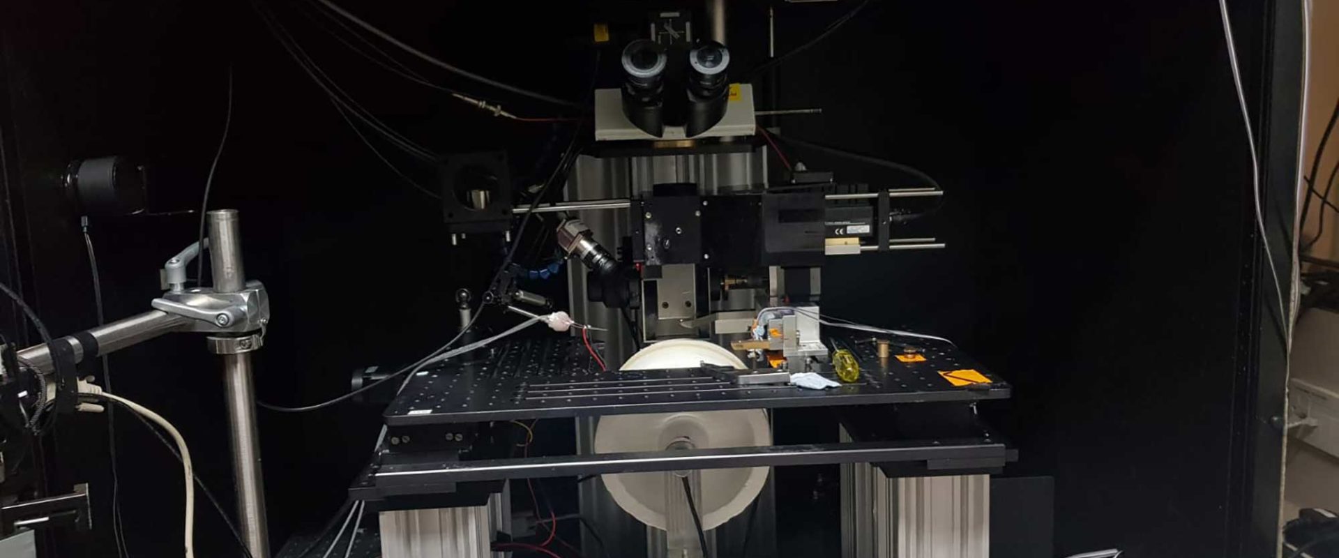
The next stage was sectioning, and I was able to use a ultramicrotome to cut our thin slices from the plastic moulds. The ultramicrotome prevented our samples from moving and it made it easier to cut. We used a diamond knife to cut which is very expensive. The thin slices floated onto water within a triangle shaped boat. The slices were so thin we had to use the idea of surface tension by using an individual hair to pick the slices up and place them onto the slide. Therefore I realised how delicate our samples are and I needed to have a steady hand. Also we had to ensure the slices were slow cuts rather than fast because that would provides us with a smooth surface.
We put some thin sections onto copper grids which needed to go in the TEM. For the SEM we did a Serial BlockFace Scanning Electron Microscope SBF-SEM, which is when the block is cut in the microscope and each time a new cut is made the section that is shown is imaged by back scatter – however, there was a disadvantage with this technique of not being able to look at our previous section. We put these sections onto silicon chips.


The next process was coating and we used a coating machine to coat a single layer of metal on our sample therefore creating the best electrical conductivity for when we place it in the SEM & TEM. The favourite part of my placement was being able to capture amazing images from all the work me and my supervisor had put in. Also from this experience it made me more excited for my career in science.
